- 您现在的位置:买卖IC网 > Sheet目录3862 > PIC16C711-04/P (Microchip Technology)IC MCU OTP 1KX14 A/D 18DIP
92
7593L–AVR–09/12
AT90USB64/128
12. External interrupts
The External Interrupts are triggered by the INT7:0 pin or any of the PCINT7..0 pins. Observe
that, if enabled, the interrupts will trigger even if the INT7:0 or PCINT7..0 pins are configured as
outputs. This feature provides a way of generating a software interrupt.
The Pin change interrupt PCI0 will trigger if any enabled PCINT7:0 pin toggles. PCMSK0 Regis-
ter control which pins contribute to the pin change interrupts. Pin change interrupts on PCINT7
..0 are detected asynchronously. This implies that these interrupts can be used for waking the
part also from sleep modes other than Idle mode.
The External Interrupts can be triggered by a falling or rising edge or a low level. This is set up
as indicated in the specification for the External Interrupt Control Registers – EICRA (INT3:0)
and EICRB (INT7:4). When the external interrupt is enabled and is configured as level triggered,
the interrupt will trigger as long as the pin is held low. Note that recognition of falling or rising
edge interrupts on INT7:4 requires the presence of an I/O clock, described in “System clock and
clock options” on page 40. Low level interrupts and the edge interrupt on INT3:0 are detected
asynchronously. This implies that these interrupts can be used for waking the part also from
sleep modes other than Idle mode. The I/O clock is halted in all sleep modes except Idle mode.
Note that if a level triggered interrupt is used for wake-up from Power-down, the required level
must be held long enough for the MCU to complete the wake-up to trigger the level interrupt. If
the level disappears before the end of the Start-up Time, the MCU will still wake up, but no inter-
rupt will be generated. The start-up time is defined by the SUT and CKSEL Fuses as described
12.0.1
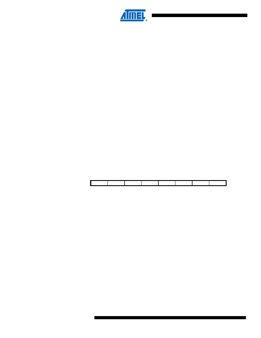
EICRA – External Interrupt Control Register A
The External Interrupt Control Register A contains control bits for interrupt sense control.
Bits 7..0 – ISC31, ISC30 – ISC00, ISC00: External Interrupt 3 - 0 Sense Control bits
The External Interrupts 3 - 0 are activated by the external pins INT3:0 if the SREG I-flag and the
corresponding interrupt mask in the EIMSK is set. The level and edges on the external pins that
activate the interrupts are defined in Table 12-1. Edges on INT3..INT0 are registered asynchro-
nously. Pulses on INT3:0 pins wider than the minimum pulse width given in Table 12-2 will
generate an interrupt. Shorter pulses are not guaranteed to generate an interrupt. If low level
interrupt is selected, the low level must be held until the completion of the currently executing
instruction to generate an interrupt. If enabled, a level triggered interrupt will generate an inter-
rupt request as long as the pin is held low. When changing the ISCn bit, an interrupt can occur.
Therefore, it is recommended to first disable INTn by clearing its Interrupt Enable bit in the
EIMSK Register. Then, the ISCn bit can be changed. Finally, the INTn interrupt flag should be
cleared by writing a logical one to its Interrupt Flag bit (INTFn) in the EIFR Register before the
interrupt is re-enabled.
Bit
7
65
43
21
0
ISC31
ISC30
ISC21
ISC20
ISC11
ISC10
ISC01
ISC00
EICRA
Read/write
R/W
Initial value
00
发布紧急采购,3分钟左右您将得到回复。
相关PDF资料
PIC18LF26K22-I/SP
IC PIC MCU 64KB FLASH 28SPDIP
PIC18F25K80-I/SP
MCU PIC 32KB FLASH 28SDIP
DSPIC33FJ12MC201-I/SS
IC DSPIC MCU/DSP 12K 20SSOP
PIC16LF628-04I/P
IC MCU FLASH 2KX14 COMP 18DIP
PIC16C716-04I/P
IC MCU OTP 2KX14 A/D PWM 18DIP
PIC18F26K22-I/SP
IC PIC MCU 64KB FLASH 28SPDIP
PIC18F45J11-I/PT
IC PIC MCU FLASH 32KB 44-TQFP
PIC24HJ12GP201-I/SO
IC PIC MCU FLASH 12KB 18SOIC
相关代理商/技术参数
PIC16C711-04/P
制造商:Microchip Technology Inc 功能描述:IC 8BIT CMOS MCU 16C711 DIP18
PIC16C711-04/SO
功能描述:8位微控制器 -MCU 1.75KB 68 RAM 13 I/O 4MHz SOIC18 RoHS:否 制造商:Silicon Labs 核心:8051 处理器系列:C8051F39x 数据总线宽度:8 bit 最大时钟频率:50 MHz 程序存储器大小:16 KB 数据 RAM 大小:1 KB 片上 ADC:Yes 工作电源电压:1.8 V to 3.6 V 工作温度范围:- 40 C to + 105 C 封装 / 箱体:QFN-20 安装风格:SMD/SMT
PIC16C711-04/SO
制造商:Microchip Technology Inc 功能描述:8BIT CMOS MCU SMD 16C711 SOIC18
PIC16C711-04/SS
功能描述:8位微控制器 -MCU 1.75KB 68 RAM 13 I/O 4MHz SSOP20 RoHS:否 制造商:Silicon Labs 核心:8051 处理器系列:C8051F39x 数据总线宽度:8 bit 最大时钟频率:50 MHz 程序存储器大小:16 KB 数据 RAM 大小:1 KB 片上 ADC:Yes 工作电源电压:1.8 V to 3.6 V 工作温度范围:- 40 C to + 105 C 封装 / 箱体:QFN-20 安装风格:SMD/SMT
PIC16C711-04E/P
功能描述:8位微控制器 -MCU 1.75KB 68 RAM 13 I/O 4MHz Ext Temp PDIP18 RoHS:否 制造商:Silicon Labs 核心:8051 处理器系列:C8051F39x 数据总线宽度:8 bit 最大时钟频率:50 MHz 程序存储器大小:16 KB 数据 RAM 大小:1 KB 片上 ADC:Yes 工作电源电压:1.8 V to 3.6 V 工作温度范围:- 40 C to + 105 C 封装 / 箱体:QFN-20 安装风格:SMD/SMT
PIC16C711-04E/SO
功能描述:8位微控制器 -MCU 1.75KB 68 RAM 13 I/O 4MHz Ext Temp SOIC18 RoHS:否 制造商:Silicon Labs 核心:8051 处理器系列:C8051F39x 数据总线宽度:8 bit 最大时钟频率:50 MHz 程序存储器大小:16 KB 数据 RAM 大小:1 KB 片上 ADC:Yes 工作电源电压:1.8 V to 3.6 V 工作温度范围:- 40 C to + 105 C 封装 / 箱体:QFN-20 安装风格:SMD/SMT
PIC16C711-04E/SS
功能描述:8位微控制器 -MCU 1.75KB 68 RAM 13 I/O 4MHz Ext Temp SSOP20 RoHS:否 制造商:Silicon Labs 核心:8051 处理器系列:C8051F39x 数据总线宽度:8 bit 最大时钟频率:50 MHz 程序存储器大小:16 KB 数据 RAM 大小:1 KB 片上 ADC:Yes 工作电源电压:1.8 V to 3.6 V 工作温度范围:- 40 C to + 105 C 封装 / 箱体:QFN-20 安装风格:SMD/SMT
PIC16C711-04I/P
功能描述:8位微控制器 -MCU 1.75KB 68 RAM 13 I/O 4MHz Ind Temp PDIP18 RoHS:否 制造商:Silicon Labs 核心:8051 处理器系列:C8051F39x 数据总线宽度:8 bit 最大时钟频率:50 MHz 程序存储器大小:16 KB 数据 RAM 大小:1 KB 片上 ADC:Yes 工作电源电压:1.8 V to 3.6 V 工作温度范围:- 40 C to + 105 C 封装 / 箱体:QFN-20 安装风格:SMD/SMT